-
 Project Curve Tracer - Schematic Creation
- Date Wed 10 February 2016
- By Jason Jones
- Category curve-tracer
- Tags curve-tracer curve tracer pic24 project
In the last post, we talked about the component selection. In this post, we will make all connections of the schematic and fill in the details that we skipped.
High-Level Design
I believe that it is often instructive to make a high-level block diagram:
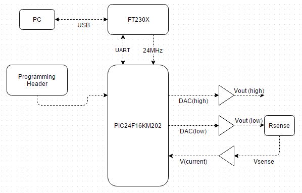
There is obviously going to be more detail than this, but this reveals our high-level design. There will be a PIC24F16KM202 which takes care of all user I/O and transmits the results over USB. The USB module will supply a 24MHz clock to the PIC. Two of the amplifiers shown will reside within the PIC and the current-sense amplifier will reside outside of that.
Output Stage
The two internal amplifiers will be connected in the voltage follower configuration and will serve to output the signal that is to go to the device under test. Vout(high) and Vout(low) will be measured using the PIC ADC in order to determine the differential voltage across the device under test.
The low-side will actually be run through what is known as a current sense resistor. Remember back to Ohm's Law:
V = IR
When we are trying to measure current, one technique is to take advantage of Ohm's Law by placing a known resistance in series with the return current. The voltage across that resistor is directly proportional to the current flowing through it:
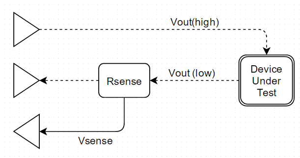
The diagram above shows the direction of current flow when the differential voltage is positive using the dotted lines. When the differential voltage is negative, the current will change directions in the dotted line, but still follow the same path.
Current-Sense Strategy
Sensing current can be very difficult, especially small currents. Fortunately, we should be able to amplify/attenuate the signal without too much impact using Rsense and the gain on the differential amplifier.
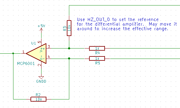
The gain is adjusted by adjusting the ratio of R4:R3 and R5:R2. It is best to make R3 = R2 and R4 = R5. Once this balance is achieved, it is a simple matter of choosing the gain value. In this case, my gain is:
R3/R4 = 10k/1k = 10
Any voltage coming in on the input lines (from the right) will be amplified by a factor of 10 and pass out to the left.
One unexplained node is the upper node going off screen from R3. This is the 'reference' voltage. In most circuits, this node is simply grounded in order to make the reference ground. in our case, we want to sense current in both positive and negative directions. If we ground this node, we will not be able to sense currents below 0. We will raise this node to a different voltage for this purpose. Even better, we will raise this node using an extra PWM output as a DAC so that we can precisely tune the reference voltage.
USB Connection
The USB connection will be nearly identical to that recommended by the FT230X datasheet. Our only modification is that we will change the CBUS0 output so that it will output a 24MHz precision clock for our microcontroller.
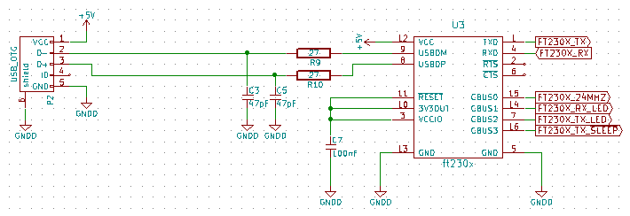
No surprises here.
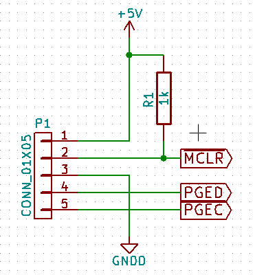
Programming Header
The standard Microchip programming header uses an RJ12 connector (phone). This is large and relatively expensive. We are going to change this to a 5-pin single row header that we don't have to populate in any production order. This is simple and easy.
The Microcontroller
This is where all of the magic happens. There are some conventions I used that you should be aware of:
- HZ = High-Z, or 'high impedance'
- LZ = Low-X, or 'low impedance'
- LD - load
The rest of the labels should make some level of sense.
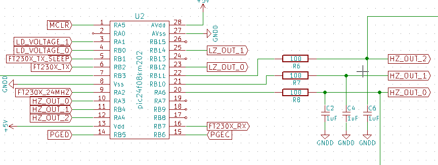
There are three RC filters to the right. These are PWM outputs. HZ_OUT_0 will go into the reference of our current-sense differential amplifier. HZ_OUT_1 will be unused (at this time) and HZ_OUT_2 will be used for biasing transistors and MOSFETs for testing. We had the extra outputs, may as well connect them to something. Note also that the HX_OUT_x pins are all going into A/D converters on the right side. This allows us to close the loop around a particular voltage and adjust as needed in order to get higher precision from these outputs.
The LZ_OUT_x pins are the voltage follower pins. They will go through some small protective resistance before driving the load.
Full Schematic
To see a full schematic with all of the pieces connected, checkout the github repository.
Some of the resistance values are very likely to change and some of them aren't as likely. This is a decent first guess and we can adjust resistance values as we learn more about our application!
Our next post will be with the layout. With so few components, that should be a breeze. At that point, we will also upload something semi-useful to github so that you can download and criticize. Enjoy!
- article
- current-sensor
- curve-tracer
- dispatch
- fan-controller
- fixed-point-math
- load-cell-sensor
- meta
- reference


 RSS
RSS
2
assembly
5
buffer
31
c
3
current sensor
28
curve tracer
2
fan controller
6
fixed-point math
4
interrupt
3
KiCAD
3
labview
5
layout
6
msp430
4
pelican
18
pic24
29
project
12
python
2
Q1.15
4
schematic
10
serial
3
solidworks
2
task manager
2
theme
3
tkinter
9
uart
9
xc16