-
 Project Curve Tracer - Setting Up PWM as a DAC
- Date Mon 29 February 2016
- By Jason Jones
- Category curve-tracer
- Tags curve-tracer c curve tracer fixed-point math pic24 Q1.15 xc16
Intro
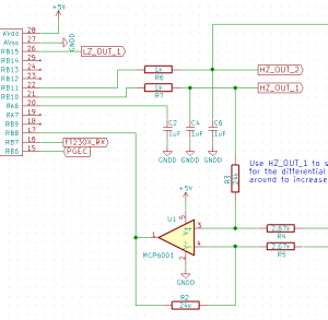
In the initial schematic, you will recall that U1 is an opamp in the differential configuration. This means that the voltage at the reference input will be the 'center' or '0' voltage of the output. We decided to place a small RC filter at the input of that opamp so that we could adjust the center of the output as needed. We are using the DACs available for a different portion of the project, so we are going to do this using the PWM through an RC circuit in order to generate the DC reference.
More Rework
Opamp Gain
Originally, I had the gain setting resistors of the opamp at 1kΩ and 10kΩ. As it turns out, I didn't have any 10k resistors in this package laying around. I modified the schematic with a ratio that was close, going with 2.67kΩ and 24kΩ for a gain of 8.99. We will probably modify this on the next round so that the resistors on the board have more common values, but this will do for now.
High-Impedance Output
Originally, we had pin 20 generating the DC bias PWM for the current sense opamp.
Since our pin 20 was taken up by a capacitor due to a misread, we had
to cut a trace and re-route to the analog out that is labeled
'HZ_OUT_1'. Fortunately, we weren't using this for anything else, so
that worked perfectly.
Opamp Output
Finally, due to the same misread, we had to cut a trace to pin 7 (see previous post) and re-route the opamp output to a different analog input. We chose pin 17.
RC Filter

We are using one of the most basic elements of electronics, the RC filter, to generate a DC signal using a variable AC waveform. By tuning the values of R, C, and the PWM frequency, we can ensure that the output is a nearly perfect DC value. In this case, we have chosen a 1kΩ resistor and a 1μF capacitor in the 'low-pass' configuration, meaning that the filter will pass the low frequency components of the input waveform. The 'cutoff' frequency occurs at:
fc = 1/(2 * pi * R * C)
In our case, this works out to 159Hz. Generally, if you want to filter all if your AC components, you stay well above the cutoff frequency, so above 1.59kHz should do quite well.
Our PWM requirement, which will go into Vin of the low-pass filter, is to have a frequency higher than 1.59kHz.
Coding
This PWM module is quite flexible, which means that it can be complex to set up. Couple that with a somewhat vague datasheet and you can spend hours setting it up. Fortunately, there are some things that are common to all PWM modules that make it fairly straightforward once you identify the registers to modify.
- Setup DIO
- Identify the PWM module and registers to modify
- Set up the time base
- Set the PWM mode
- Turn on the module
- Modify the duty cycle as required
Setup DIO
The digital pins RB10 and RB11 must be setup as digital outputs using the TRISB bits.
Identify PWM/CCP Modules
In our case, we are using pins 21 and 22 of the microcontroller. This means that we have access to PWM pins OC1C and OC2A. Re-interpreting these values, we have Output Compare on PWM Module 1, output C and Output Compare on PWM module 2, output A. This identifies that we will be setting up two different output compare modules, OC1 and OC2. This will guide us through the rest of our setup.
When we are setting up OC1 and we see in the datasheet "CCPxCON1L", substitute the number '1' for the 'x'. For our application, nearly all registers are the same for the two modules.
Time Base
The timer in this PWM module is capable operating in 16-bit or 32-bit mode. We only need 16-bits for our time base, so we clear the T32 bit in the CCP1CON1L and CCP2CON1L. We have no need to adjust the prescaler for the timer, so leave the prescaler at '1'.
For our period register, CCPxPRL, we only need to stay above 1.59kHz. Additionally, we would like to have the ability to adjust with a reasonable degree of precision - say, 10 bits - so we will set this value to 1024 (2 \^ 10).
Tcycle = 1/16000000 = 62.5ns
Tpwm = Tcycle * 1024 = 64μs
Fpwm = 1/Tpwm = 15.625kHz
This is well above our minimum desired frequency and will make a great starting point.
PWM Mode
The datasheet can be confusing on some of the specifics of the PWM module, but just remember that the 'default' operation is often close to where you want to be.
In our case, the mode we want is 'Dual Edge Compare Mode, buffered'. What this means is that, as the counter counts up, it will at some point encounter the value stored in CCPxRA at which time the pin value will go 'high'. When the timer value reaches the value stored in CCPxRB, the pin will go 'low'. We don't need to adjust both edges, so we will leave CCPxRA = 0 and adjust CCPxRB when we want to change the duty cycle. More on that later.
Turn On Module
Once all of the registers are set up, turn on the module!
Complete Module Setup
The complete module setup code is:
1 2 3 4 5 6 7 8 9 10 11 12 13 14 15 16 17 18 19 20 21 22 23 24 25 26 | void initPwm(void){
// use OC1C (pin 21, RB10) and OC2A (pin 22, RB11)
TRISBbits.TRISB10 = TRISBbits.TRISB11 = DIO_DIGITAL;
/* Initialize MCCP module
* */
/* period registers */
CCP1PRH = CCP2PRH = 0;
CCP1PRL = CCP2PRL = 1024;
CCP1CON1L = CCP2CON1L = 0x0005;
CCP1CON1H = CCP2CON1H = 0x0000;
CCP1CON2L = CCP2CON2L = 0x0000;
CCP1CON2H = 0x8400; // enable output OC1C
CCP2CON2H = 0x8100; // enable output 0C2A
CCP1CON3L = CCP2CON3L = 0; // dead time disabled
CCP1CON3H = CCP2CON3H = 0x0000;
CCP1CON1Lbits.CCPON = CCP2CON1Lbits.CCPON = 1;
/* duty cycle registers */
CCP1RA = CCP2RA = 0;
CCP1RB = CCP2RB = 0;
return;
}
|
Note that the vast majority of bits are '0'. Also note that the only difference betweeen CCP1 and CCP2 is with regard to the specific output number - A on CCP2 and C on CCP1 - on register CCPxCON2H. All other registers are identical.
Modify Duty Cycle
To modify the duty cycle, we only need to modify the CC2RB value. For this type of application, I generally like to abstract the interface a bit and use Q1.15 as the input to the function abstraction. This makes other operations later much simpler, such as implementing a PID loop.
We will call our new functions 'setDutyCycleHZ1' and 'setDutyCycleHZ2'. The functions are nearly identical and will take a Q1.15 number as the sole parameter and, based on the contents of the period register, setup the CCPxRB register appropriately.
1 2 3 4 5 6 7 8 9 | void setDutyCycleHZ1(q15_t dutyCycle){
CCP1RB = q15_mul(dutyCycle, CCP1PRL);
return;
}
void setDutyCycleHZ2(q15_t dutyCycle){
CCP2RB = q15_mul(dutyCycle, CCP2PRL);
return;
}
|
Testing
In main, we initialize HZ1 with a 50% duty cycle and HZ2 with a 25% duty cycle in Q1.15 format:
1 2 3 | /* set the initial duty cycle */
setDutyCycleHZ1(16384);
setDutyCycleHZ2(8192);
|
Looking at the HZ2 output:

The yellow trace is the PWM and the blue trace is the output of the RC filter. Note the slight fluctuation on the DC output waveform. We can set our scope to AC coupled and measure that small fluctuation more closely:

According to our measurements of the output when we AC-couple the signal and change the vertical scale to 20mV/division, we can measure the peak-to-peak voltage to be (35.2mV - (-32.0mV)) = 67.2mV. This is acceptable for the moment. We know that we can reduce from here by one of three strategies:
- Increase the resistance of the RC network
- Increase the capacitance of the RC network
- Increase the PWM frequency
As we move through the project, we may notice that 67.2mV is simply too much fluctuation enough for whatever reason.
- article
- current-sensor
- curve-tracer
- dispatch
- fan-controller
- fixed-point-math
- load-cell-sensor
- meta
- reference


 RSS
RSS
2
assembly
5
buffer
31
c
3
current sensor
28
curve tracer
2
fan controller
6
fixed-point math
4
interrupt
3
KiCAD
3
labview
5
layout
6
msp430
4
pelican
18
pic24
29
project
12
python
2
Q1.15
4
schematic
10
serial
3
solidworks
2
task manager
2
theme
3
tkinter
9
uart
9
xc16